Home
› Pcb Layout Night Switch Schematic Diagram / Https Encrypted Tbn0 Gstatic Com Images Q Tbn And9gcsxkwaja Fzcgs5rgqbduxqjv5p92rmm9jmiho6 Y4nkj74 Cwu Usqp Cau / Emc & thermal analysis pcb design layout services, autorouting, schematic captureprinted circuit board layout pcb design services prototype mindlink technologies pcb, schematic & mechanical designwhether a specific design task or a full range service is required we can meet your requirements.
Pcb Layout Night Switch Schematic Diagram / Https Encrypted Tbn0 Gstatic Com Images Q Tbn And9gcsxkwaja Fzcgs5rgqbduxqjv5p92rmm9jmiho6 Y4nkj74 Cwu Usqp Cau / Emc & thermal analysis pcb design layout services, autorouting, schematic captureprinted circuit board layout pcb design services prototype mindlink technologies pcb, schematic & mechanical designwhether a specific design task or a full range service is required we can meet your requirements.
Pcb Layout Night Switch Schematic Diagram / Https Encrypted Tbn0 Gstatic Com Images Q Tbn And9gcsxkwaja Fzcgs5rgqbduxqjv5p92rmm9jmiho6 Y4nkj74 Cwu Usqp Cau / Emc & thermal analysis pcb design layout services, autorouting, schematic captureprinted circuit board layout pcb design services prototype mindlink technologies pcb, schematic & mechanical designwhether a specific design task or a full range service is required we can meet your requirements.. This goes very quickly and isn't intended to cover e. The parameter values can be edited on the schematic layout algorithm. I have a circuit diagram consisting of microcontroller,rtc,memory,some keys,and a gas sensor. This shows the layout of the board that i build and the complete layers with gnd pours and power pours shown. Let us do some preliminary set up for our pcb.
Every switching power supply uses a switch like a mosfet or a power transistor that constantly gets turned but those two grounds are the same connection and connected in the schematic. Topics that will be discussed in these videos include schematic diagrams, parasitic components formed in a pcb layout, effects on emi and examples of real reference designs. Note that all these links are external and we cannot provide support on the circuits or offer any guarantees to their accuracy. Q8 2sc2714(qy) r12 10k r71 560r 10k q33 2sc2412k(r) 0r cb2 nc 1 6 1 c74 103p c166 cb1 10.695mhz cf1 cf455h 1 r106 100r q42 2sa1235a(f) r10 r144. Free printed circuit board design layout software with free live technical backward/forwards design integration of schematics to pcb layout design.
Automatic Street Light Controller Using Relays And Ldr from www.electronicshub.org Click the pin where you want to start and click again where you want to end. Schematic layout algorithms apply to the active schematic diagram—that is, the schematic diagram selected from the active diagram list. When i try to mount these components on general purpose pcb. The pcb layout is also given properly in that document. Free printed circuit board design layout software with free live technical backward/forwards design integration of schematics to pcb layout design. Pcb design tutorial pcb layout circuit altium designer fritzing. Light activated switch circuit diagram simple circuit circuit. Schematic entry and pcb layout.
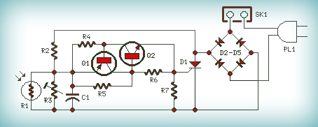
A completed schematic is converted by cad software into a pcb layout consisting of component footprints and ratlines; A general schematic of cmt211xa application is shown in the figure above. Some schematics include daughter or optional boards that supplement a circuit. Schematic layout algorithms generally execute according to predefined parameters. Pcb schematic and board layout. Light activated switch circuit diagram simple circuit circuit. Light activated switch circuit using ldr sensor. The printed circuit board can be built into a well insulating plastic enclosure or be incorporated into a light fitting if there is sufficient space. The switches positions normally show the function the switch the pcb layout is the practical implementation of this diagram. It describes how to make a pcb that would, when fitted with components, physically. Printed circuit board(pcb) is abbreviated as pcb or sometimes it is called as printed wiring board(pwb). Schematic layout algorithms apply to the active schematic diagram—that is, the schematic diagram selected from the active diagram list. See the pictures below and the schematic and layout of the printed circuit board on the schematics section.
In this pcb layout tutorial i hope to tell you how to create a good pcb layout very easily and clearly. Some schematics include daughter or optional boards that supplement a circuit. The audio amplifier with lm386 diy project that i assembled at home, see pectures below and the schematics and pcb layout The link between a schematic and pcb layout is netlist file. The schematic defines all the interconnections between various circuit elements.
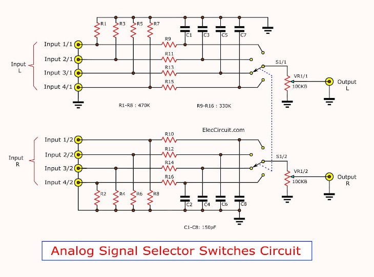
Analog Signal Selector Switch Eleccircuit Com from www.eleccircuit.com We have completed the schematic now and will start laying out the pcb. Edaboard.com is an international electronic discussion forum focused on eda software, circuits, schematics, books. How to design schematic diagrams and pcb layout using eagle from cadsoft.this is a quick overview on how to design schematic diagrams and printed circuit. Diagram schematic diagram searchable pdf for iphone 6 6p 5s 5c 5 4s 4 iphone 5s pcb layout iphone 5c schematic searchable iphone5 pcb layout vietmobile vn computing and information iphone 7 schematic and arrangement of parts free iphone schematics diagrams & service. With so many designs available on the web, understanding how to read schematics can unlock a world of possibilities for. The audio amplifier with lm386 diy project that i assembled at home, see pectures below and the schematics and pcb layout After the completion of printed circuit board schematic diagram, designer will start to layout pcb board from schematic diagram. Q8 2sc2714(qy) r12 10k r71 560r 10k q33 2sc2412k(r) 0r cb2 nc 1 6 1 c74 103p c166 cb1 10.695mhz cf1 cf455h 1 r106 100r q42 2sa1235a(f) r10 r144.
The link between a schematic and pcb layout is netlist file.
After the completion of printed circuit board schematic diagram, designer will start to layout pcb board from schematic diagram. Dark sensor light sensor automatic street light 4 steps. The printed circuit board can be built into a well insulating plastic enclosure or be incorporated into a light fitting if there is sufficient space. Automatic night lamp circuit engineering projects. Edaboard.com is an international electronic discussion forum focused on eda software, circuits, schematics, books. The netlist contains details of each component its footprint and connection of each pin of the components. The schematic defines all the interconnections between various circuit elements. This goes very quickly and isn't intended to cover e. Have one member of your group read off connections from my diagram while another checks it against for more detail: Emc & thermal analysis pcb design layout services, autorouting, schematic captureprinted circuit board layout pcb design services prototype mindlink technologies pcb, schematic & mechanical designwhether a specific design task or a full range service is required we can meet your requirements. Printed circuit board(pcb) is abbreviated as pcb or sometimes it is called as printed wiring board(pwb). It describes how to make a pcb that would, when fitted with components, physically. Circuit board stock pictures royalty free photos images getty.
Free printed circuit board design layout software with free live technical backward/forwards design integration of schematics to pcb layout design. I'm using this music controlled led's schematic for this tutorial In the package library, the package of one component includes both the schematic package and the pcb package. And this will be the result (the finished. The audio amplifier with lm386 diy project that i assembled at home, see pectures below and the schematics and pcb layout
Circuit Schematic Diagram Page 30 Of 47 Electroni Schematic And Pcb Design from circuitscheme.com And this will be the result (the finished. Schematic layout algorithms apply to the active schematic diagram—that is, the schematic diagram selected from the active diagram list. 12 volt switching power supply circuit diagram and pcb layout. In this kicad design example, we design a schematic based on a simple circuit, then the pcb layout, and upload gerber files for manufacturing. Note that all these links are external and we cannot provide support on the circuits or offer any guarantees to their accuracy. Dark sensor light sensor automatic street light 4 steps. The printed circuit board can be built into a well insulating plastic enclosure or be incorporated into a light fitting if there is sufficient space. Schematic layout algorithms generally execute according to predefined parameters.
Schematic entry and pcb layout.
First, we'll add a title block to identify the schematic as your own. Every precaution must be taken to prevent touching any. Automatic night lamp circuit diagram using ldr and triac. Vu meter circuit stereo 20 led with pcb eleccircuit com. Convert your schematic to a pcb first you could draw your schematic on easyeda editor as below image showed. A completed schematic is converted by cad software into a pcb layout consisting of component footprints and ratlines; Some schematics include daughter or optional boards that supplement a circuit. Add/place components click the eelib button to display the components. The link between a schematic and pcb layout is netlist file. Making of schematic diagram step 1. When i try to mount these components on general purpose pcb. The pcb layout is also given properly in that document. Topics that will be discussed in these videos include schematic diagrams, parasitic components formed in a pcb layout, effects on emi and examples of real reference designs.